
Delayer
EquipmentRIE, Mechanical & Chemical
An analytical technique used to observe the inner layers of the semiconductor die by removing its various metal layers and oxide films.
Introduction
Semiconductors consist of various layers of metal and oxide. If each layer needs to be removed to learn its structure and conduct analysis, delayering is performed. The inner layers can be removed one by one by wet etching using chemicals, dry etching using gas, and polishing using physicochemical techniques.
Application
Aluminum layer etch, Copper layer etch, Silicon oxidation layer etch, Polysilicon layer etch, Layered etching of semiconductor compositions and semiconductor defect analysis, Reverse engineering
The Equipment
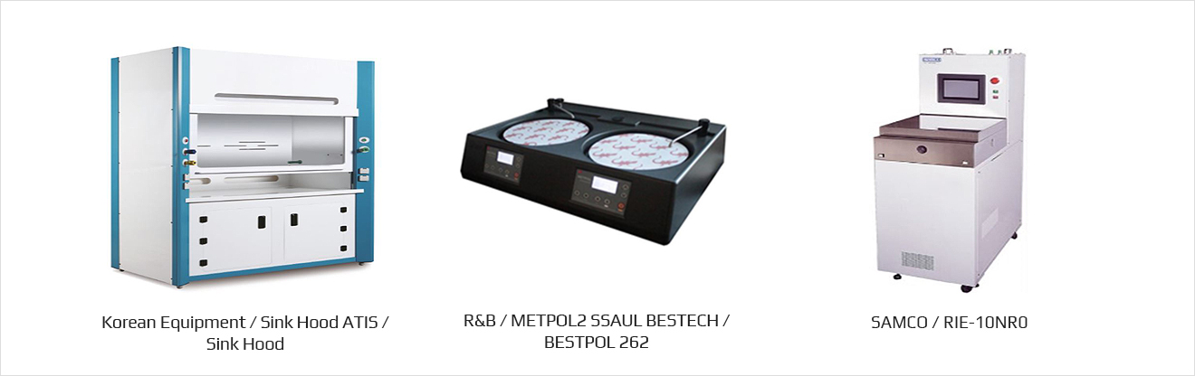
Controlled acid etching
Can remove the multi-layer structure of the chip
Have different approaches (ion etching / chemical etching / mechanical polishing)
Technical Use Case
Layer by Layer De-layer
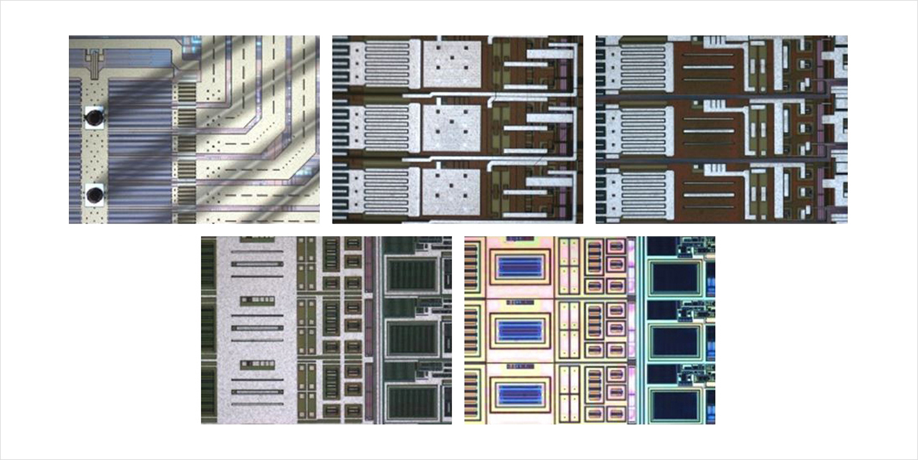
Failure Analysis : De-layer
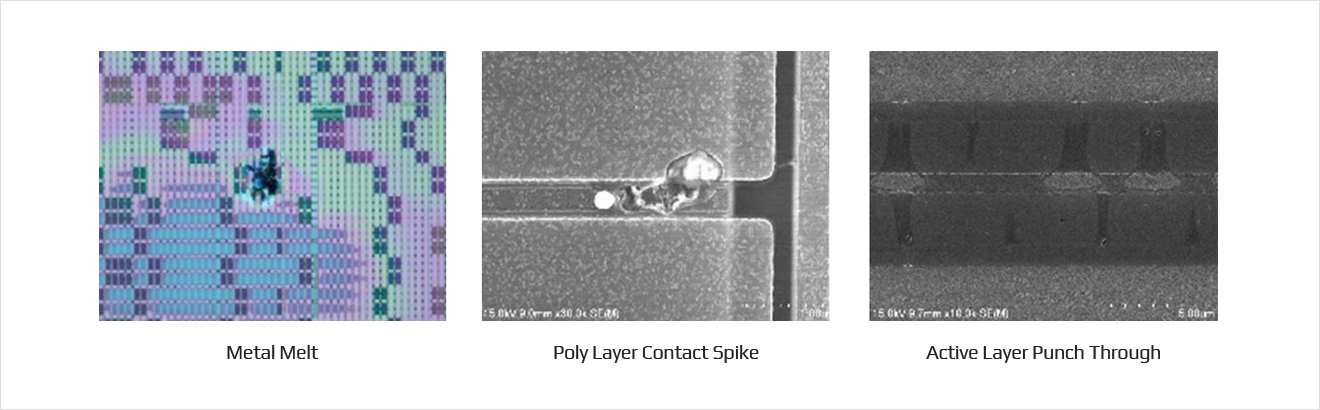
Contact Point
Person in charge- • TEL.
- 010-6400-8094
- • E-mail.
- ec.fa@qrtkr.com